- 您现在的位置:买卖IC网 > Sheet目录366 > TMDXEVM5515 (Texas Instruments)EVAL MODULE DSP FOR C55XX
�� ��
��
��SPRS645F� –� AUGUST� 2010� –� REVISED� OCTOBER� 2013�
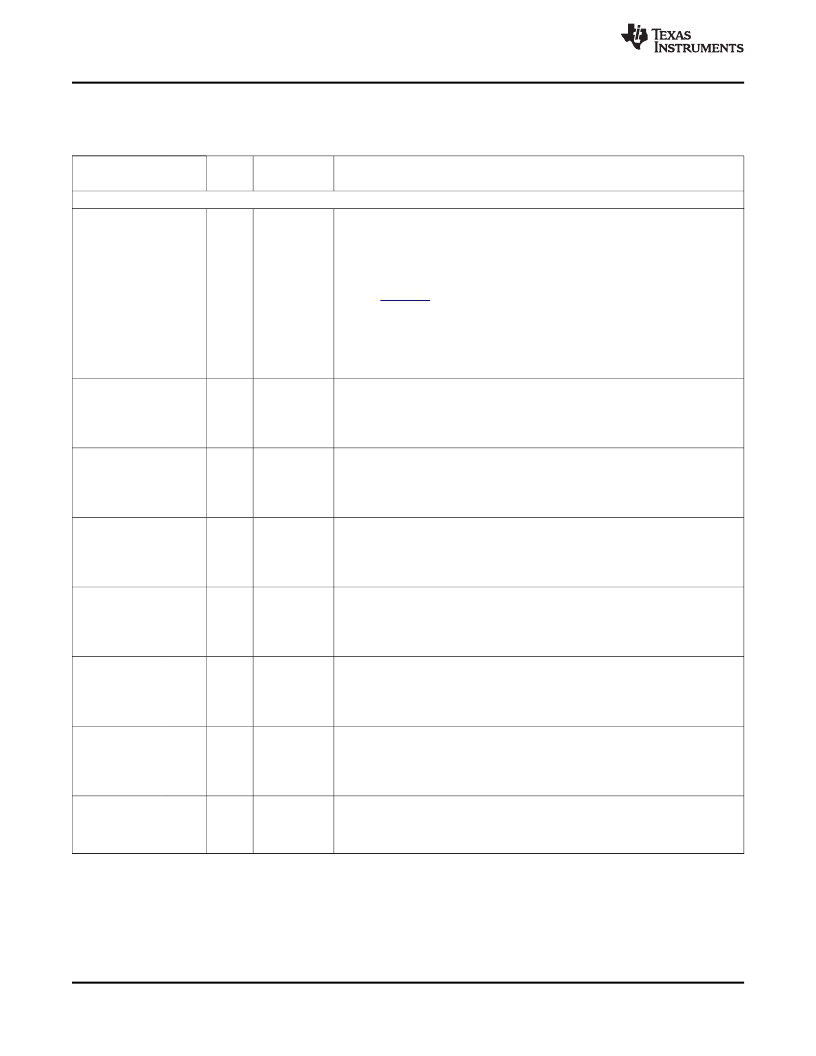
�2.5.13� GPIO� Terminal� Functions�
�Table� 2-18.� GPIO� Terminal� Functions�
��SIGNAL�
�NAME�
�NO.�
�TYPE� (1)�
�(2)�
�OTHER� (3)�
�(4)�
�DESCRIPTION�
�General-Purpose� Input/Output�
�External� Flag� Output.� XF� is� used� for� signaling� other� processors� in� multiprocessor�
�configurations� or� XF� can� be� used� as� a� fast� general-purpose� output� pin.�
�XF� is� set� high� by� the� BSET� XF� instruction� and� XF� is� set� low� by� the� BCLR� XF�
�instruction� or� by� writing� to� bit� 13� of� the� ST1_55� register.� For� more� information� on� the�
�–�
�ST1_55� register,� see� the� TMS320C55x� 3.0� CPU� Reference� Guide� (literature�
�XF�
�M8�
�O/Z�
�DV� DDIO�
�number:� SWPU073� ).�
�BH�
�For� XF� pin� behavior� at� reset,� see� Section� 5.7.2� ,� Pin� Behaviors� at� Reset� .�
�Note:� This� pin� may� consume� static� power� if� configured� as� Hi-Z� and� not� externally�
�pulled� low� or� high.� Prevent� current� drain� by� externally� terminating� the� pin.� XF� pin� is�
�ONLY� in� the� Hi-Z� state� when� doing� boundary� scan.� Therefore,� external� termination�
�is� probably� not� required� for� most� applications.�
�This� pin� is� multiplexed� between� MMC0,� I2S0,� and� GPIO.�
�MMC0_CLK/�
�I2S0_CLK/�
�GP[0]�
�L10�
�I/O/Z�
�IPD�
�DV� DDIO�
�BH�
�For� GPIO,� it� is� general-purpose� input/output� pin� 0� (GP[0]).�
�Mux� control� via� the� SP0MODE� bits� in� the� EBSR.� The� IPD� resistor� on� this� pin� can� be�
�enabled� or� disabled� via� the� PDINHIBR1� register.�
�This� pin� is� multiplexed� between� MMC0,� I2S0,� and� GPIO.�
�MMC0_CMD/�
�I2S0_FS/�
�GP[1]�
�M11�
�I/O/Z�
�IPD�
�DV� DDIO�
�BH�
�For� GPIO,� it� is� general-purpose� input/output� pin� 1� (GP[1]).�
�Mux� control� via� the� SP0MODE� bits� in� the� EBSR.� The� IPD� resistor� on� this� pin� can� be�
�enabled� or� disabled� via� the� PDINHIBR1� register.�
�This� pin� is� multiplexed� between� MMC0,� I2S0,� and� GPIO.�
�MMC0_D0/�
�I2S0_DX/�
�GP[2]�
�L9�
�I/O/Z�
�IPD�
�DV� DDIO�
�BH�
�For� GPIO,� it� is� general-purpose� input/output� pin� 2� (GP[2]).�
�Mux� control� via� the� SP0MODE� bits� in� the� EBSR.� The� IPD� resistor� on� this� pin� can� be�
�enabled� or� disabled� via� the� PDINHIBR1� register.�
�This� pin� is� multiplexed� between� MMC0,� I2S0,� and� GPIO.�
�MMC0_D1/�
�I2S0_RX/�
�GP[3]�
�M10�
�I/O/Z�
�IPD�
�DV� DDIO�
�BH�
�For� GPIO,� it� is� general-purpose� input/output� pin� 3� (GP[3]).�
�Mux� control� via� the� SP0MODE� bits� in� the� EBSR.� The� IPD� resistor� on� this� pin� can� be�
�enabled� or� disabled� via� the� PDINHIBR1� register.�
�This� pin� is� multiplexed� between� MMC0� and� GPIO.�
�MMC0_D2/�
�GP[4]�
�L12�
�I/O/Z�
�IPD�
�DV� DDIO�
�BH�
�For� GPIO,� it� is� general-purpose� input/output� pin� 4� (GP[4]).�
�Mux� control� via� the� SP0MODE� bits� in� the� EBSR.� The� IPD� resistor� on� this� pin� can� be�
�enabled� or� disabled� via� the� PDINHIBR1� register.�
�This� pin� is� multiplexed� between� MMC0� and� GPIO.�
�MMC0_D3/�
�GP[5]�
�L11�
�I/O/Z�
�IPD�
�DV� DDIO�
�BH�
�For� GPIO,� it� is� general-purpose� input/output� pin� 5� (GP[5]).�
�Mux� control� via� the� SP0MODE� bits� in� the� EBSR.� The� IPD� resistor� on� this� pin� can� be�
�enabled� or� disabled� via� the� PDINHIBR1� register.�
�MMC1_CLK/�
�IPD�
�This� pin� is� multiplexed� between� MMC1,� I2S1,� and� GPIO.�
�I2S1_CLK/�
�GP[6]�
�M13�
�I/O/Z�
�DV� DDIO�
�BH�
�For� GPIO,� it� is� general-purpose� input/output� pin� 6� (GP[6]).�
�Mux� control� via� the� SP1MODE� bits� in� the� EBSR.�
�(1)�
�(2)�
�(3)�
�(4)�
�I� =� Input,� O� =� Output,� Z� =� High� impedance,� S� =� Supply� voltage,� GND� =� Ground,� A� =� Analog� signal,� BH� =� Bus� Holder�
�Input� pins� of� type� I,� I/O,� and� I/O/Z� are� required� to� be� driven� at� all� times.� To� achieve� the� lowest� power,� these� pins� must� not� be� allowed� to�
�float.� When� they� are� configured� as� input� or� high-impedance� state,� and� not� driven� to� a� known� state,� they� may� cause� an� excessive� IO-�
�supply� current.� Prevent� this� current� by� externally� terminating� it� or� enabling� IPD/IPU,� if� applicable.�
�IPD� =� Internal� pulldown,� IPU� =� Internal� pullup.� For� more� detailed� information� on� pullup/pulldown� resistors� and� situations� where� external�
�pullup/pulldown� resistors� are� required,� see� Section� 3.8.1� ,� Pullup/Pulldown� Resistors� .�
�Specifies� the� operating� I/O� supply� voltage� for� each� signal�
�38�
�Device� Overview�
��Product� Folder� Links:� TMS320C5515�
�Copyright� ?� 2010–2013,� Texas� Instruments� Incorporated�
�发布紧急采购,3分钟左右您将得到回复。
相关PDF资料
TMDXEXP1808L
KIT EXPERIMENTER FOR AM180X
TO263-3EV-VREG
BOARD EVAL TO220-3/TO263-3 VREG
TO263-5EV-VREG
EVAL BOARD VREG TO220-5/TO263-5
TOOLSTICK-EK
KIT TOOL EVAL SYS IN A USB STICK
TPS23757EVM
EVALUATION MODULE FOR TPS23757
TPS62230EVM-370
EVAL MODULE FOR TPS62230-370
TRAVELCUBE
SURGE SUP 1OUT W/RJ11 DIRECTPLUG
TRAVELER100BT
SURGE SUP 2OUT W/RJ11 DIRECTPLUG
相关代理商/技术参数
TMDXEVM5515
制造商:Texas Instruments 功能描述:TMS320C5515 DSP Evaluation Module
TMDXEVM642
制造商:Texas Instruments 功能描述:Tools Development kit For Use
TMDXEVM6424
功能描述:开发板和工具包 - TMS320 C6424 DSP Eval Mod RoHS:否 制造商:Texas Instruments 产品:Experimenter Kits 工具用于评估:F2802x 核心:TMS320 接口类型:UART, USB 工作电源电压:
TMDXEVM6446
制造商:Rochester Electronics LLC 功能描述:DAVINCI EVM BUNDLE W/O EMULATOR - Bulk 制造商:Texas Instruments 功能描述:DAVINCI EVM BUNDLE W/O EMULATOR - Bulk
TMDXEVM6446T
制造商:Texas Instruments 功能描述:DM6446 DIGITAL VIDEO EVALUATION MODULE - Boxed Product (Development Kits)
TMDXEVM6446TS
制造商:Texas Instruments 功能描述:DM6446 DIGITAL VIDEO EVALUATION MODULE - Trays
TMDXEVM6452
功能描述:开发板和工具包 - TMS320 C6452 EVM Evaluation Module RoHS:否 制造商:Texas Instruments 产品:Experimenter Kits 工具用于评估:F2802x 核心:TMS320 接口类型:UART, USB 工作电源电压:
TMDXEVM6455
功能描述:开发板和工具包 - TMS320 C6455 Evaluation Module RoHS:否 制造商:Texas Instruments 产品:Experimenter Kits 工具用于评估:F2802x 核心:TMS320 接口类型:UART, USB 工作电源电压: